Shift Registers: Serial and Parallel Data Transfer
Introduction
Imagine you're sending a text message. Your phone doesn't send all the characters at once—it converts them to binary and sends them one bit at a time over the air. At the receiving end, those bits must be collected and converted back into parallel data for processing. This is exactly what shift registers do!
A shift register is a sequential circuit that stores and moves data, either serially (one bit at a time) or in parallel (all bits simultaneously). They're fundamental to:
- Serial communication (UART, SPI, I2C)
- Data storage and buffering
- Time delay generation
- Parallel-to-serial and serial-to-parallel conversion
- Digital signal processing
- Sequence generation
If counters are the "clocks" of digital systems, shift registers are the "conveyor belts"—moving data from one place to another, converting between serial and parallel formats along the way.
What is a Shift Register?
A shift register is a cascade of flip-flops where the output of one flip-flop feeds the input of the next. On each clock pulse, data "shifts" from one flip-flop to the next.
Basic Structure:
- Multiple flip-flops in series (usually D flip-flops)
- Common clock signal
- Data shifts through on each clock edge
- Can shift left, right, or both directions
Shift Register vs Counter:
| Feature | Shift Register | Counter |
|---|---|---|
| Purpose | Move/store data | Count pulses |
| Connection | Serial cascade | Feedback logic |
| Output | Shifted data | Binary count |
| Application | Data transfer | Timing/counting |
Classification of Shift Registers
Shift registers are classified by their input/output methods:
Shift Registers
├── Serial-In Serial-Out (SISO)
├── Serial-In Parallel-Out (SIPO)
├── Parallel-In Serial-Out (PISO)
├── Parallel-In Parallel-Out (PIPO)
└── Bidirectional (Left/Right)
Naming Convention:
- First term: How data enters (Serial or Parallel)
- Second term: How data exits (Serial or Parallel)
Serial-In Serial-Out (SISO) Shift Register
The Simplest Shift Register
SISO is the most basic type: data enters serially and exits serially.

Operation:
- Data bit enters at serial input
- On each clock pulse, each bit shifts one position right
- After N clock pulses (N = number of FFs), first bit appears at output
SISO Timing Diagram Example
Shifting binary 1011 through 4-bit SISO:

State Table:
| CLK | Input | Q0 | Q1 | Q2 | Q3 (Output) |
|---|---|---|---|---|---|
| 0 (initial) | - | 0 | 0 | 0 | 0 |
| 1 | 1 | 1 | 0 | 0 | 0 |
| 2 | 0 | 0 | 1 | 0 | 0 |
| 3 | 1 | 1 | 0 | 1 | 0 |
| 4 | 1 | 1 | 1 | 0 | 1 |
Key Points:
- Data takes N clock cycles to propagate through N-bit register
- Acts as a time delay: output is delayed by N clock cycles
- Used for temporary data storage and delay lines
SISO Applications
1. Time Delay
Signal → SISO (N bits) → Delayed Signal (by N clock cycles)
Used in: Digital signal processing, echo effects
2. Serial Data Transmission
Data → SISO → Serial Line → SISO → Recovered Data
Used in: Simple communication protocols
3. Data Buffering
Fast source → SISO → Slow destination
Provides timing isolation
Serial-In Parallel-Out (SIPO) Shift Register
Serial to Parallel Conversion
SIPO accepts data serially and outputs all bits simultaneously in parallel.
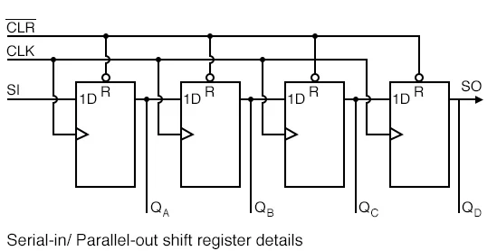
Operation:
- Serial data enters bit by bit
- After N clock pulses, all N bits are stored in parallel
- All bits available simultaneously at outputs
SIPO Timing Diagram Example
Loading 1011 into 4-bit SIPO:

State Progression:
| CLK | Input | Q3 | Q2 | Q1 | Q0 | Parallel Data |
|---|---|---|---|---|---|---|
| 0 | - | 0 | 0 | 0 | 0 | 0000 |
| 1 | 1 | 0 | 0 | 0 | 1 | 0001 |
| 2 | 0 | 0 | 0 | 1 | 0 | 0010 |
| 3 | 1 | 0 | 1 | 0 | 1 | 0101 |
| 4 | 1 | 1 | 0 | 1 | 1 | 1011 ✓ |
SIPO Applications
1. Serial Communication Receivers
Serial data stream → SIPO → Parallel byte → Microcontroller
Example: UART receiver converting serial bits to 8-bit byte
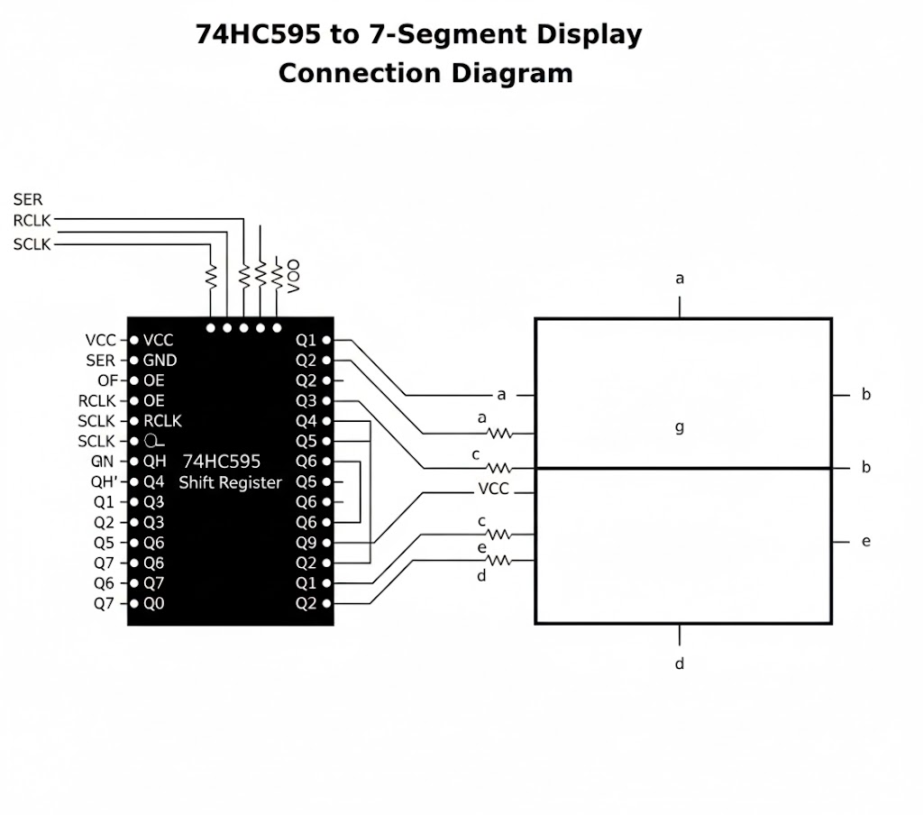
2. LED/Display Drivers
Serial command → SIPO → Parallel LED control
Reduces number of I/O pins needed
Example: 74HC595 driving 8 LEDs with 3 wires (data, clock, latch)
3. Data Expansion
Microcontroller (few pins) → SIPO → Many parallel outputs
Used to expand I/O capability
Commercial IC Example: 74HC164
- 8-bit SIPO shift register
- Serial input, 8 parallel outputs
- Clear input
- Simple and commonly used
Using SIPO, you can control 8 outputs with just 2-3 pins (serial data + clock + optional latch) instead of 8 pins! This is why they're popular in LED matrices and 7-segment displays.
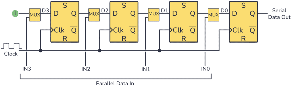
Parallel-In Serial-Out (PISO) Shift Register
Parallel to Serial Conversion
PISO accepts data in parallel and outputs it serially, one bit at a time.

Control Signals:
- LOAD/SHIFT̄: Select operation mode
- LOAD=1: Load parallel data into all FFs
- LOAD=0: Shift data serially
- Clock: Triggers load or shift operation
PISO Operation
Two-Phase Operation:
Phase 1: Parallel Load (SHIFT/LOAD̄ = 1)
- All parallel inputs (D0-D3) loaded into FFs simultaneously
- Takes one clock pulse
Phase 2: Serial Shift (SHIFT/LOAD̄ = 0)
- Data shifts out serially, one bit per clock
- Takes N clock pulses for N-bit register
PISO Timing Diagram Example
Loading 1011 and shifting out:

State Table:
| CLK | Mode | D3 D2 D1 D0 (in) | Q3 Q2 Q1 Q0 | Serial Out |
|---|---|---|---|---|
| 0 | LOAD | 1 0 1 1 | 1 0 1 1 | - |
| 1 | SHIFT | - | 0 1 0 1 | 1 |
| 2 | SHIFT | - | 0 0 1 0 | 1 |
| 3 | SHIFT | - | 0 0 0 1 | 0 |
| 4 | SHIFT | - | 0 0 0 0 | 1 |
 |
PISO Applications
1. Serial Communication Transmitters
Microcontroller (parallel byte) → PISO → Serial transmission
Example: UART transmitter sending 8-bit data serially
2. Keyboard Scanning
Multiple keys (parallel) → PISO → Serial data to CPU
Reduces wiring complexity
3. Parallel Bus to Serial Conversion
8-bit parallel data bus → PISO → Single serial wire
Useful when transitioning between systems
Commercial IC Example: 74HC165
- 8-bit PISO shift register
- Parallel load capability
- Serial output
- Complementary serial output (Q̄)
Parallel-In Parallel-Out (PIPO) Shift Register
Simple Parallel Storage
PIPO is essentially a parallel register—data loaded in parallel, available in parallel.

Operation:
- All data loaded simultaneously on clock edge
- All data available simultaneously at outputs
- No serial shifting involved

PIPO Applications
1. Data Registers
Storage element in CPUs, buffers, FIFOs
2. Timing Synchronization
Capture snapshot of multiple signals simultaneously
Ensure all bits sampled at same time
3. Pipeline Registers
Used in pipelined processors to store intermediate results
PIPO shift registers are what we typically call "registers" in digital systems. The CPU's accumulator, program counter, and data registers are all essentially PIPO structures.
Bidirectional Shift Register
Shifting in Both Directions
Bidirectional (or universal) shift registers can shift data left OR right based on control signal.
Control Modes:
| S1 | S0 | Operation |
|---|---|---|
| 0 | 0 | Hold (no shift) |
| 0 | 1 | Shift Right |
| 1 | 0 | Shift Left |
| 1 | 1 | Parallel Load |
Operation:
- Shift Right: Data moves Q3→Q2→Q1→Q0, serial input enters Q3
- Shift Left: Data moves Q0→Q1→Q2→Q3, serial input enters Q0
- Hold: All outputs maintain current value
- Parallel Load: All inputs loaded simultaneously
Bidirectional Timing Example

Bidirectional Applications
1. Arithmetic Operations
Shift left = Multiply by 2
Shift right = Divide by 2
Used in ALUs for fast arithmetic
2. Bidirectional Communication
Data can flow in either direction based on protocol
3. Rotational Encoders
Detect direction of rotation (left vs right shift)
Commercial IC Example: 74HC194
- 4-bit universal shift register
- Parallel load
- Right shift, left shift, hold modes
- Asynchronous clear
- Very versatile!
Universal Shift Register (74HC194)
The 74HC194 is the most flexible shift register IC—it can do everything!
Mode Selection Table:
| CLR̄ | S1 | S0 | Operation |
|---|---|---|---|
| 0 | X | X | Clear (async) |
| 1 | 0 | 0 | Hold |
| 1 | 0 | 1 | Shift Right |
| 1 | 1 | 0 | Shift Left |
| 1 | 1 | 1 | Parallel Load |
Applications of 74HC194:
- UART implementation: Can be configured as SIPO or PISO
- Ring counters: Connect output back to input
- Sequence generators: Create custom bit patterns
- General-purpose data manipulation
The 74HC194 is like the Swiss Army knife of shift registers—one IC can replace multiple specialized ones. Keep it in your component library!
Special Shift Register Configurations
Ring Counter (Recirculating Shift Register)
Configuration: Connect serial output back to serial input.
Operation:
- Single '1' circulates through register
- After N clocks, pattern repeats (N = number of stages)
State Sequence:
| CLK | Q3 | Q2 | Q1 | Q0 |
|---|---|---|---|---|
| 0 | 0 | 0 | 0 | 1 |
| 1 | 0 | 0 | 1 | 0 |
| 2 | 0 | 1 | 0 | 0 |
| 3 | 1 | 0 | 0 | 0 |
| 4 | 0 | 0 | 0 | 1 |
Applications:
- Stepper motor control: Sequential activation of coils
- State machines: Simple sequential control
- LED chasers: Moving light patterns
Johnson Counter (Twisted Ring Counter)
Configuration: Connect inverted output back to input.
Operation:
- Alternating pattern of 0s and 1s shifts through
- Modulus = 2N (twice the number of stages!)
State Sequence:
| CLK | Q3 | Q2 | Q1 | Q0 | Pattern |
|---|---|---|---|---|---|
| 0 | 0 | 0 | 0 | 0 | |
| 1 | 0 | 0 | 0 | 1 | |
| 2 | 0 | 0 | 1 | 1 | |
| 3 | 0 | 1 | 1 | 1 | |
| 4 | 1 | 1 | 1 | 1 | |
| 5 | 1 | 1 | 1 | 0 | |
| 6 | 1 | 1 | 0 | 0 | |
| 7 | 1 | 0 | 0 | 0 | |
| 8 | 0 | 0 | 0 | 0 | (repeats) |
Advantages:
- MOD-8 counter using only 4 flip-flops!
- No decoding glitches
- Self-starting (recovers from errors)
Linear Feedback Shift Register (LFSR)
Configuration: Feedback using XOR gates creates pseudo-random sequence.
Properties:
- Generates maximal-length sequence: 2^N - 1 unique states
- Appears random but is deterministic
- Same seed produces same sequence
Applications:
- Pseudo-random number generation: Test patterns, simulations
- CRC (Cyclic Redundancy Check): Error detection in communication
- Scrambling/Descrambling: Data encryption
- Built-in self-test (BIST): Testing digital circuits
Example LFSR Sequence (4-bit with taps at Q3, Q2):
0001 → 0010 → 0100 → 1000 → 0011 → 0110 → 1100 → 1011 → 0101 → 1010 → 0111 → 1110 → 1111 → 1101 → 1001 → (back to 0001)
Total: 15 unique states (2^4 - 1)
LFSRs are used in many encryption algorithms (though not strong enough alone). They're also used in GPS satellites for spreading codes and in cell phone communication!
Practical Shift Register Applications
Application 1: Serial Communication (UART)
Transmitter (PISO):
8-bit parallel data → PISO shift register → Serial output (TX)
Receiver (SIPO):
Serial input (RX) → SIPO shift register → 8-bit parallel data

Application 2: LED Matrix Display
Common Configuration:
- SIPO (74HC595) controls columns (8 bits)
- Another SIPO controls rows (8 bits)
- Total: 64 LEDs controlled with 3 wires!
Control Scheme:
Microcontroller (3 pins):
- Serial Data (DS)
- Clock (SHCP)
- Latch (STCP)
↓
Multiple 74HC595 ICs cascaded
↓
8×8 LED Matrix
Advantages:
- Massive pin savings: 3 pins control 64 LEDs
- Can cascade indefinitely (limited by update rate)
- Simple software control
Application 3: Keyboard Matrix Scanning (74HC165)
Configuration:
- PISO (74HC165) reads keyboard rows
- Microcontroller scans columns
- Parallel key states converted to serial
Scanning Process:
1. Activate column 1
2. Load all row states into PISO
3. Shift out serially to read which keys pressed
4. Repeat for all columns
Application 4: Delay Line for Digital Audio
Setup:
- Long shift register (hundreds to thousands of stages)
- Audio sample enters serially
- Delayed audio exits after N clock cycles
Echo Effect:
Original signal ────→ (+) ───→ Output with echo
                      ↑
Shift register (delay) ─┘
Application 5: Data Acquisition System
Multi-Channel ADC Readout:
8 analog inputs → MUX → ADC → PISO → Serial to CPU
Benefits:
- Single ADC serves multiple channels
- Serial transmission reduces wiring
- Cost-effective data acquisition
Shift Register Timing Considerations
Clock Frequency Limits
Maximum Clock Frequency:
Where:
- t_pd = Propagation delay through flip-flop
- t_su = Setup time
- t_hold = Hold time
Example:
- 74HC164 (SIPO): f_max ≈ 50 MHz @ 5V
- 74HC595 (SIPO with latch): f_max ≈ 40 MHz @ 5V
Cascading Shift Registers
When cascading multiple shift registers:
Total Propagation Delay:
Example:
- Cascading 4× 8-bit shift registers = 32 bits total
- Per-stage delay: 10 ns
- Total delay: 32 × 10 ns = 320 ns
- Max update rate: ~3 MHz
Very long shift register chains can become slow. For high-speed applications, consider parallel loading with shorter serial segments.
Shift Register ICs Summary
| IC | Type | Bits | Features |
|---|---|---|---|
| 74HC164 | SIPO | 8 | Serial in, parallel out, clear |
| 74HC165 | PISO | 8 | Parallel in, serial out, load |
| 74HC594 | SIPO | 8 | With output register, 3-state |
| 74HC595 | SIPO | 8 | With storage register, most popular |
| 74HC597 | PISO | 8 | With input register |
| 74HC194 | Universal | 4 | Left/right shift, parallel load |
| 74HC299 | Universal | 8 | Bidirectional, 3-state outputs |
| CD4014 | PISO | 8 | CMOS, parallel/serial load |
| CD4015 | SIPO | Dual 4 | Dual 4-bit shift registers |
| CD4094 | SIPO | 8 | With strobe output |
Designing with Shift Registers
Design Checklist
1. Determine Requirements:
- Serial or parallel input?
- Serial or parallel output?
- Number of bits needed?
- Clock frequency?
- Need bidirectional shifting?
2. Select IC:
- Choose appropriate type (SISO/SIPO/PISO/Universal)
- Verify voltage compatibility (3.3V vs 5V)
- Check speed specifications
- Consider pin count
3. Circuit Design:
- Add decoupling capacitors (0.1µF near each IC)
- Include pull-up/pull-down resistors on unused inputs
- Plan cascade connections if needed
- Add LED indicators for debugging
4. Software Control:
- Define timing parameters (setup, hold times)
- Implement serial protocol (if applicable)
- Add error checking (parity, CRC)
- Test with boundary cases
Troubleshooting Shift Registers
Common Problems
Problem 1: Data Not Shifting
- Check: Clock signal present?
- Check: Clock edges clean (no bouncing)?
- Check: Enable/load signals correct?
- Verify: Power supply stable
Problem 2: Incorrect Data Output
- Check: Serial input signal quality
- Check: Clock and data timing (setup/hold violations)
- Check: Proper ground connections
- Test: Slow down clock frequency
Problem 3: Intermittent Operation
- Check: Decoupling capacitors present and close to IC
- Check: Wire lengths (long wires = more noise)
- Check: Temperature (ICs may fail at extremes)
- Verify: All inputs driven (no floating pins)
Debug Techniques
1. Slow Clock Testing:
- Reduce frequency to ~1 Hz
- Visually observe with LEDs
- Manually verify each shift operation
2. Logic Analyzer:
- Capture all signals simultaneously
- Verify timing relationships
- Identify glitches or violations
3. Loopback Test:
- Connect output back to input
- Verify data circulates correctly
- Isolates input vs output problems
Summary
Shift registers are versatile circuits that move and store data:
✅ SISO: Serial delay lines
✅ SIPO: Serial to parallel conversion (receivers)
✅ PISO: Parallel to serial conversion (transmitters)
✅ PIPO: Simple parallel storage (registers)
✅ Bidirectional: Flexible shift direction
Key Takeaways:
- Pin Savings: Control many outputs with few pins
- Format Conversion: Bridge serial and parallel worlds
- Timing: Shift registers create precise delays
- Versatility: Ring, Johnson, LFSR configurations
- Universal ICs: 74HC194/299 do everything
Now we understand how to move and store data. Next, we'll learn how to add and subtract binary numbers—the foundation of arithmetic logic units (ALUs) in processors!
Further Reading
- Datasheets: 74HC595, 74HC165, 74HC194
- Application notes on cascading shift registers
- Arduino libraries for shift register control
- LFSR theory for advanced sequences
Practice Problems:
- Design a 16-bit SIPO using two 74HC164 ICs
- Calculate data rate for 8-bit serial transmission at 1 MHz clock
- How many 74HC595s needed to drive 32 LEDs?
- Design ring counter for 6-state sequence
- Calculate maximum clock frequency for 3-stage cascaded 74HC164 (tpd=25ns each)
- Implement 8-bit PISO using 74HC165 for keyboard scanning
- Design LFSR-based random number generator (4-bit)