Ferrite Beads — The Tiny Components That Silently Fix EMI Problems
Ferrite beads appear on almost every professional PCB, and almost no student-project PCB. This one fact tells you everything about the gap between a prototype and a product. They cost ₹2–5 each, occupy less than 2 mm², and are invisible to the untrained eye — but a switching regulator without one on its output is an unlicensed FM transmitter waiting to happen.
What a Ferrite Bead Actually Is
A ferrite bead is a lossy inductor. That distinction — lossy — is what makes it different from a regular inductor. A regular inductor stores energy and returns it to the circuit. A ferrite bead absorbs high-frequency energy and converts it to heat. Not much heat — we are talking microwatts — but that energy is gone from your circuit instead of bouncing around and causing interference.
Physically, a ferrite bead is made of ferrite material: iron oxide (Fe₂O₃) combined with ceramic binders such as manganese or zinc oxide, pressed and sintered into a bead shape. In chip form (the dominant type in modern electronics), it looks identical to a 0402 or 0603 resistor. The lossy magnetic properties of the ferrite are what create the frequency-dependent impedance.
The Impedance vs Frequency Curve
This is the most important concept in ferrite bead selection, and most engineers gloss over it.
At DC and low-frequency AC, the bead has near-zero impedance. It passes DC current freely — this is what you want on a power rail. As frequency rises into the MHz range, the bead behaves like an inductor: impedance rises steeply (proportional to frequency). Then, above a characteristic frequency, the ferrite material becomes lossy: the inductance converts to resistance, and that resistance dissipates the energy as heat rather than returning it.
A representative curve for a Murata BLM18AG601SN1:
| Frequency | Impedance | Character |
|---|---|---|
| 1 kHz | < 1 Ω | Resistive (DCR only) |
| 1 MHz | ~20 Ω | Inductive |
| 10 MHz | ~150 Ω | Inductive + resistive |
| 100 MHz | ~600 Ω | Resistive (lossy — energy dissipated) |
| 1 GHz | ~200 Ω | Resistive (falling — ferrite saturates) |
The headline spec — "600 Ω at 100 MHz" — is always measured at 100 MHz with a 100 mA test current. Your actual circuit conditions may differ.
Three Parameters You Must Check in Every Datasheet
1. Impedance at 100 MHz (Z@100MHz)
The headline number. Higher is better for suppression, but do not chase the highest number blindly — check the frequency curve to confirm peak impedance falls where your noise actually is. A bead rated 600 Ω at 100 MHz may only be 100 Ω at 500 MHz if that is where your noise lives.
2. DC Resistance (DCR)
The bead is in series with your power rail. Its DC resistance causes a real voltage drop:
V_drop = I_load × DCR
A bead with 500 mΩ DCR powering a 200 mA load drops 100 mV. If your regulator is set to 3.3V and your IC needs 3.0V minimum, this matters. Typical DCR ranges: 50 mΩ (large, low-impedance beads) to 600 mΩ (small, high-impedance beads). Pick the lowest DCR that gives sufficient impedance.
3. Rated DC Current (I_rated)
Ferrite is a magnetic material. At high DC current, it saturates — the magnetic domains align and cannot respond to the AC noise anymore. Impedance collapses. The rated current is the current at which impedance drops to a specified fraction (typically 80%) of the nominal value. Always derate by 20–30%.
Placement Rules
On Power Lines
Place the bead in series, between the power supply output and the IC VCC pin. The bead plus the decoupling capacitors on the IC side form a low-pass filter:
- Bead = series impedance element
- 100 nF ceramic capacitor on IC side = shunt element to ground
- Together: low-pass π-section that attenuates high-frequency noise from both directions
Do not place the bead between the capacitor and the IC. The capacitor must be on the IC side of the bead, close to the IC.
On Signal Lines
Use small-value ferrite beads (e.g., Murata BLM15AG121SN1, 120 Ω at 100 MHz) in series on noisy digital output lines driving into an analog section. Place as close to the noise source as possible — not at the victim end.
On USB and Ethernet Lines — Common-Mode Ferrites
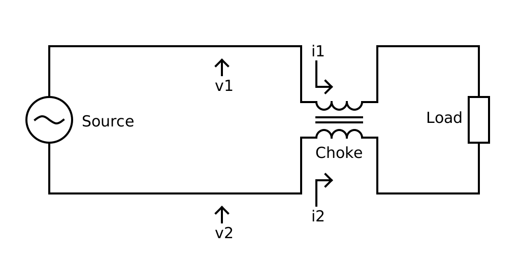
Common-mode choke: differential signals pass through (fields cancel), common-mode noise is blocked (fields add). Source: Wikimedia Commons, CC BY-SA

A standard ferrite bead kills differential signals along with the noise. For differential pairs (USB, Ethernet, CAN), use a common-mode choke: a single component with two windings wound in opposing directions on a shared ferrite core.
- Differential signal: sees two opposing magnetic fields → they cancel → near-zero impedance → signal passes through unaffected
- Common-mode noise: sees two aiding magnetic fields → high impedance → noise is blocked
Example: TDK ACM2012-900-2P-T (900 Ω at 100 MHz, 100 mA, for USB 2.0 full-speed lines).
Power Rail Filter Circuit
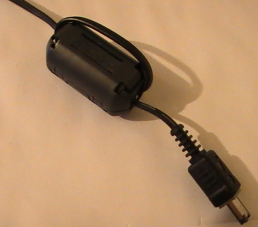
Ferrite bead low-pass filter: the bead (series impedance) plus bypass capacitors on the IC side form an LC-style low-pass filter that keeps switching noise off the power rail. Source: Wikimedia Commons, CC BY-SA

This is the standard pattern for filtering a noisy power rail before an MCU or RF IC:
The 100 nF ceramic handles frequencies from 1 MHz to ~500 MHz. The 100 µF bulk cap handles load transients at lower frequencies. Together, they provide a low-impedance shunt path at the IC pins for any noise that gets past the bead, AND a charge reservoir so the IC can draw burst current without pulling VCC down.
Worked Selection Example
Scenario: STM32G0 MCU running at 3.3V, drawing 80 mA peak during active GPIO toggling. Switching regulator noise at 2 MHz and harmonics up to 200 MHz.
Requirements: Need ≥ 100 Ω impedance from 10 MHz to 200 MHz. Voltage drop < 50 mV. Saturation current margin > 2×.
Selection: Murata BLM18AG601SN1
- Z @ 100 MHz: 600 Ω ✓
- DCR: 300 mΩ
- Rated current: 500 mA
Voltage drop: 80 mA × 300 mΩ = 24 mV — acceptable, leaves 3.276 V at IC ✓
Saturation margin: 500 mA rated vs 80 mA peak = 6.25× margin ✓
Result: part confirmed. Order from LCSC (C76729) at ~₹3 each.
Common Mistakes
Too high DCR on high-current rails. A 1 Ω DCR bead on a 500 mA rail drops 500 mV. Your regulator now needs to compensate and your IC may brown-out under load. Always calculate V_drop = I × DCR before committing to a part.
Peak impedance at the wrong frequency. A bead labelled 1000 Ω might peak at 25 MHz and be only 200 Ω at 100 MHz. Look at the curve in the datasheet, not just the headline number. Murata SimSurfing, TDK Product Center, and Würth REDEXPERT all provide interactive impedance curves.
Bead on the wrong side of the noise source. The bead must be between the noise source and the victim, not between the victim and elsewhere. If your MCU is the noise source contaminating an ADC, the bead goes on the VCC trace close to the MCU — not anywhere else.
Using a standard ferrite bead on a differential pair. It will attenuate the signal. Use a common-mode choke.
Common Ferrite Bead Series — Quick Reference
| Part Number | Series | Z @ 100 MHz | Max Current | DCR | Best For |
|---|---|---|---|---|---|
| Murata BLM18AG601SN1 | BLM18AG | 600 Ω | 500 mA | 300 mΩ | MCU power rails |
| Murata BLM21PG221SN1 | BLM21PG | 220 Ω | 3 A | 22 mΩ | Power supply output |
| TDK MPZ1608S601A | MPZ1608 | 600 Ω | 200 mA | 400 mΩ | Signal lines |
| Würth 742792510 | WE-CBF | 510 Ω | 1 A | 120 mΩ | General purpose |
| TDK ACM2012-900-2P-T | ACM | 900 Ω (CM) | 100 mA | — | USB 2.0 lines |
| TDK ACM7060-701-2PL-TL | ACM7060 | 700 Ω (CM) | 3 A | — | Ethernet, CAN |
PCB Layout Considerations for Ferrite Beads
Ferrite beads are series components — layout matters as much as part selection.
Keep the bead close to the noise source, not close to the victim. The noisy power rail from a switching regulator should hit the bead before it fans out to other parts of the board. Once noise is on the power plane, you cannot un-spread it.
Short, direct connections. Any extra trace length between the bead and its associated decoupling capacitors adds parasitic inductance and undermines the filter formed between them. Target < 3 mm between bead and capacitor.
Do not share vias. The shunt capacitor on the IC side of the bead must have its own dedicated via to ground. A via shared with another noisy component is a coupling path that partially negates the bead.
Package size vs frequency. Smaller ferrite bead packages (0402, 0201) have lower parasitic capacitance and maintain higher impedance at GHz frequencies compared to larger 0805 packages. For applications above 500 MHz, choose 0402 or smaller.
Thermal considerations. The bead dissipates absorbed energy as heat. At full rated current, a small 0402 bead handling 500 mA can reach 40–60°C above ambient. This is not a concern for most signal-level currents but check the thermal derating curve in the datasheet for high-current power rails.
Verifying Ferrite Bead Effectiveness
After placing beads on your PCB, verification is straightforward with a near-field probe and spectrum analyser:
- Power the board and run a representative workload (MCU active, communication interfaces active)
- Place a small H-field loop probe 2–3 mm above the power trace on the noisy side of the bead
- Note the peak frequency and amplitude
- Move the probe to the IC side of the bead
- The peak at the noise frequency should be reduced by 20–40 dB if the bead and decoupling are properly placed
If the reduction is less than 15 dB, check: decoupling cap ground via quality, trace length between bead and cap, and whether you selected the right bead for the noise frequency.
Key Takeaway
A ferrite bead is a frequency-selective energy absorber — it passes DC, attenuates MHz-range noise. The three numbers that matter are impedance at 100 MHz, DC resistance, and rated current. Place it between the noise source and the victim, always with decoupling capacitors on the clean side. Keep the layout tight — parasitic inductance from long traces undoes the filter. Get this right and your board stops radiating. Get it wrong and you pay a test lab to tell you exactly what you missed.