Electronics Hardening — Building Hardware That Survives ESD, Surges, and the Real World
A prototype tested by its own development team in a clean lab will never see ESD. It will never see
a 1 kV surge on the power input. It will never be plugged in while a fluorescent lamp starter fires
nearby or while a 7.5 kW motor starts on the same distribution panel. A product in the field will
see all three — probably in the first week of installation. Electronics hardening is the discipline
of designing for that reality before the first unit ships, not after the first field return.
ESD — Electrostatic Discharge (IEC 61000-4-2)
A person walking across a low-humidity carpeted office builds up 2–4 kV of static charge. When they
touch a grounded metal enclosure or a connector pin, that charge discharges in under 1 ns through a
peak current of 7–20 A (human body model). The rise time of that current pulse is sub-nanosecond —
which means it contains spectral energy well into the GHz range. Unprotected IC input pins and
communication ports see this as a momentary overvoltage that can permanently damage gate oxides or
latch up CMOS structures.
IEC 61000-4-2 Test Levels
| Level | Contact Discharge | Air Discharge |
|---|---|---|
| Level 1 | ±0.5 kV | ±1 kV |
| Level 2 | ±1 kV | ±2 kV |
| Level 3 | ±2 kV | ±4 kV |
| Level 4 | ±4 kV | ±8 kV |
Consumer electronics typically targets Level 2 (±1/2 kV). Industrial equipment targets Level 3 or
Level 4. Medical equipment per IEC 60601-1-2 targets Level 4 (±8 kV air discharge to any external
surface). If your product has exposed metal connectors or a metal enclosure, assume Level 4.
ESD Protection

TVS diode symbols. Unidirectional (left) clamps one polarity; bidirectional (right) clamps both — required for data lines where the signal swings both ways. Source: Wikimedia Commons, CC BY-SA Components

TVS diode (Transient Voltage Suppressor): a unidirectional or bidirectional avalanche diode
that clamps the line voltage within nanoseconds. Key parameters: standoff voltage (must be above
normal operating voltage), clamping voltage (voltage under peak test current), and peak pulse
current (must handle the test current without degrading).
For a 3.3 V signal line: use a bidirectional TVS with standoff ≥ 3.3 V and clamping voltage below
the IC's absolute maximum input voltage. Example: PRTR5V0U2X (Nexperia) — dual-channel, 5.5 V
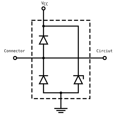
Combined TVS + rail-to-rail diode ESD protection array: clamp diodes steer transients to VCC or GND; TVS clamps VCC rail voltage. Used on USB, HDMI, and Ethernet ports. Source: Wikimedia Commons, CC BY-SA
standoff, 18 V clamp at 1 A, SOT-363 package, 0.5 pF capacitance. Low capacitance is critical for
USB and high-speed lines — high-capacitance TVS devices distort signals at 480 Mbps.

ESD protection arrays: for multi-channel interfaces (USB 3.0, HDMI 2.0, PCIe), use integrated
ESD arrays:
- TPD4E05U06 (Texas Instruments): 4-channel, 0.4 pF/channel, for USB 3.x and PCIe
- ESDA14V2L (STMicroelectronics): bidirectional, 14 V standoff, very low capacitance
- IP4220CZ6 (Nexperia): 5 V USB 2.0 ESD, 2-channel, 0.9 pF
Schottky clamp diodes: for general-purpose GPIO lines that are not high-frequency, a pair of
Schottky diodes clamping to VCC and GND (e.g., BAT54S dual Schottky, SOT-23) provides cheap
protection with low capacitance.
PCB Layout Rules for ESD
- TVS and ESD protection devices must be placed at the connector, on the line before it enters
the PCB interior. If the TVS is 5 cm away from the connector, the inductance of the trace
between connector and TVS limits the clamping speed — the full ESD pulse reaches the IC before
the TVS can respond. - Ground via for the TVS must be immediately beside the TVS pad — shortest possible return
path to the ground plane. - Traces from connector to TVS to IC must be straight — no loops, no right-angle turns that
add parasitic inductance. - Ensure a continuous ground plane under and around ESD protection components. Gaps in the
ground plane near connectors are a common PCB review failure.
Surge Protection — IEC 61000-4-5
Lightning does not have to hit your building to damage your product. A strike 1 km away couples
energy into overhead power and I/O cables. IEC 61000-4-5 defines the test waveform: 1.2/50 µs
voltage wave (1.2 µs rise, 50 µs to half-value, open circuit) combined with an 8/20 µs current
wave (8 µs rise, 20 µs to half-value, short circuit). Test levels go up to ±4 kV / ±2 kA.
Surge Protection Components
MOV (Metal Oxide Varistor): a voltage-dependent resistor that becomes low-resistance above its
clamping voltage. Very high peak current capability (kA range). Used as the primary clamp on mains
and DC power inputs.
- SIOV-S14K275 (TDK EPCOS): 14 mm disc, 275 V AC, 6.5 kA peak pulse, for European 230 V mains
- V10E150P (Littelfuse): 10 mm disc, 150 V DC, 4.5 kA, for 48 V or 110 V DC systems
MOVs degrade with each surge event — their clamping voltage drops over time. Design for MOV
replacement or use a replaceable fuse in series. MOVs can fail short-circuit under severe
overcurrent — always protect with a series fuse rated below the MOV's short-circuit current.
GDT (Gas Discharge Tube): spark gap in a sealed gas-filled enclosure. Very high voltage before
firing (150–470 V trigger), then extremely low clamping voltage once conducting. Handles very large
currents (20 kA) but has a significant follow-current problem (keeps conducting after the surge is
gone until the circuit current drops below the holding current). Use as the first stage of a
two-stage surge protector.
Typical two-stage surge protection topology for a 24 V DC industrial input:
Connector → GDT (300 V) → series current-limiting resistor or PTC → MOV (33 V) → TVS (27 V) → IC
The GDT handles the initial large surge energy. The MOV absorbs the remainder and clamps to 33 V.
The TVS performs final clamping below the IC's maximum rating.
EFT/Burst Protection — IEC 61000-4-4
EFT (Electrical Fast Transient) bursts are generated by mechanical switches, contactors, and relay
coils on the same power circuit. The characteristic waveform: individual pulses with 5 ns rise
time, 50 ns width, grouped into 15 ms bursts at 300 Hz repetition, with burst repetition at 5 kHz.
Test levels reach ±2 kV on AC power ports and ±1 kV on I/O ports for industrial equipment.
The energy content of each individual EFT pulse is low — the challenge is that thousands of pulses
arrive in rapid succession, and firmware or communication logic can misinterpret them as valid
signals (false triggering on GPIO, corrupted UART framing, I²C bus errors).
EFT Protection Techniques
X2 capacitors on mains input: safety-rated capacitors across L-N (X2 rating, 275 V AC, 0.1 µF
to 0.47 µF). They form a low-impedance path for the fast transient to the other mains conductor
before reaching the power supply. Mandatory for any mains-connected product.
Common-mode choke on DC power input: a common-mode choke (e.g., WÜRTH 744235 series or
TDK ACM series) presents high impedance to common-mode noise (both lines rising and falling
together) while passing differential current. For a 24 V DC industrial supply: a 4.7 mH
common-mode choke rated at 1–2 A.
Bulk capacitance on DC rails: 100 µF electrolytic (low-ESR, 105°C rated — use Panasonic FM or
Nippon Chemi-Con KZE series) on the DC input absorbs burst energy before it reaches sensitive ICs.
Opto-isolation on I/O lines: for digital I/O in heavy industrial environments, opto-isolators
(e.g., 6N137 for high-speed, PC817 for general-purpose) break the galvanic path between
the external world and the control electronics. No galvanic path = no EFT path. This is the
nuclear option and also the most reliable.
Decoupling Capacitors — The Most Under-Appreciated Protection
Decoupling capacitors do two things: they stabilize local supply voltage by sourcing transient
current demand locally (faster than the power supply can respond), and they provide a low-impedance
return path for high-frequency noise currents. Both functions matter for EMC.
The Three-Tier Decoupling Strategy
Tier 1 — Bulk decoupling (10–100 µF):
Low-frequency energy reservoir. Handles slow supply variations, motor starting transients, and
inrush from adjacent circuits. Use 47 µF or 100 µF low-ESR electrolytic or tantalum capacitors.
Place one per power domain, or at the entry point of each supply to a PCB region.
- Panasonic EEU-FM series (electrolytic, low ESR, 105°C)
- Kemet T491 series (tantalum, low ESR, SMD)
Tier 2 — Mid-frequency decoupling (100 nF ceramic, X7R or X5R):
Handles switching transients and digital logic switching noise (1–100 MHz range). One 100 nF
capacitor per IC VCC pin. Not per IC — per VCC pin. An STM32 with VDDA, VDD, and VDD_IO all
separate needs decoupling on each. Use 0402 X7R ceramic. Placement: within 1–2 mm of the IC VCC
pin, ground via immediately beside (not at the end of a trace, beside the capacitor pad).
Tier 3 — High-frequency decoupling (10 nF or 1 nF ceramic, C0G/NP0):
For very high-frequency noise (100 MHz+), use C0G/NP0 dielectric which maintains capacitance
value at high frequency (X7R loses 50%+ capacitance at resonance). Place 10 nF C0G between the
100 nF X7R and the IC VCC pin, or on high-frequency ICs (RF, USB PHY, Ethernet PHY) add 1 nF C0G
as well.
Power plane → 100 µF electrolytic → 100 nF X7R → 10 nF C0G → IC VCC pin
              (bulk, centrally)      (per VCC pin)   (per VCC pin, C0G)
Capacitor Placement — The Detail That Gets Ignored
A 100 nF capacitor with a 5 mm trace to the IC VCC pin and a 10 mm trace back to ground has
approximately 10–15 nH of trace inductance in its current loop. At 100 MHz, that inductance has
an impedance of 2π × 100 MHz × 12 nH ≈ 7.5 Ω. The capacitor's impedance at 100 MHz is about
0.016 Ω. The trace inductance has eliminated 99.8% of the decoupling benefit. Place the
capacitor next to the pin, ground via next to the capacitor, not at the end of a long trace.
Power Supply Filtering — Input Stage
Pi Filter Topology
The most effective passive filter for DC power inputs is the pi (π) filter: capacitor → series
inductor → capacitor. The first capacitor provides initial filtering; the inductor blocks high-
frequency noise; the second capacitor provides a low-impedance source to the load.
Vin → [C1: 100µF] → [L1: 10µH, 2A rated] → [C2: 47µF] → [IC power domain]
For SMPS (switched-mode power supply) input filtering:
- C1: 100 µF electrolytic, rated for input voltage + 20% margin
- L1: power inductor with low DCR (< 0.1 Ω), rated current > peak load current
- C2: 47 µF electrolytic + 100 nF ceramic in parallel (covers both frequency ranges)
Differential vs Common-Mode Filtering
Differential-mode noise travels on the two supply conductors in opposite directions (one line
up, one line down). Filtered by a series inductor + shunt capacitor between the conductors.
Common-mode noise travels on both conductors in the same direction relative to earth. Filtered
by a common-mode choke — wound so that differential current cancels in the core (no saturation)
while common-mode current sees high inductance.
Industrial designs almost always need both. The common-mode choke handles radiated immunity test
failures; the differential-mode filter handles conducted emissions test failures.
PCB Layout Rules for Immunity
-
Ground plane continuity — a single unbroken ground plane on the layer immediately below the
signal layer. Splits in the ground plane create high-impedance return paths that act as antennas.
The only acceptable split: between analog ground and digital ground, joined at a single controlled
point (star ground node, typically near the ADC reference pin). -
Connector placement and TVS/MOV at the entry point — protection components go at the
connector, before the signals travel further onto the board. A TVS 5 cm from the connector is
largely useless. -
Clock line routing — keep clock lines short, matched to characteristic impedance (50 Ω, use
width calculator for your stackup), terminated at the receiver. Route away from I/O connectors
and cable runs. -
Guard rings around analog circuits — a grounded copper ring (connected to analog ground at
one via) around ADC input traces and sensitive analog sections reduces common-mode noise pickup. -
Chassis ground stitch capacitors — the PCB ground plane must be connected to the metal
chassis (if present) through stitch capacitors, not direct DC connection. Use 4.7 nF, 2 kV
rated ceramic capacitors (e.g., Murata DE series), placed every 5–10 cm around the PCB edge
and near connectors. These provide a low-impedance RF connection to chassis while blocking DC
and power-frequency ground loops. Without these, the chassis and PCB ground planes are not at
the same RF potential — the chassis does not act as an RF shield. -
Return path management for high-speed signals — for USB, Ethernet, and HDMI, route
differential pairs over a continuous ground plane. Never route a high-speed pair across a plane
split or a slot in the ground plane. The return current will take the long way around the gap,
creating a large current loop that radiates.
Protection Layer — Connector to IC
Threat and Protection Reference Table
| Threat | Test Standard | Test Level (Industrial) | Protection Component | Placement Rule |
|---|---|---|---|---|
| ESD — human touch | IEC 61000-4-2 | ±4 kV contact / ±8 kV air | TVS diode, ESD array (PRTR5V0U2X) | At connector pin, GND via beside device |
| Surge — lightning induced | IEC 61000-4-5 | ±2 kV / ±1 kA (L3) | GDT + MOV + TVS (staged) | At power/IO entry, GDT first |
| EFT/Burst — switching | IEC 61000-4-4 | ±2 kV (power), ±1 kV (I/O) | X2 cap, CM choke, bulk cap | Mains: X2 cap + choke before rectifier |
| Radiated RF | IEC 61000-4-3 | 10 V/m (L3) | CM choke, decoupling, shielding | CM choke on long I/O cables |
| Conducted RF | IEC 61000-4-6 | 10 Vrms (L3) | CM choke + filter cap | At cable entry to PCB |
| Power dip | IEC 61000-4-11 | 70% dip, 25 cycles | Bulk capacitance (1000 µF+), BOD | Bulk cap at DC input |
| Magnetic field | IEC 61000-4-8 | 30 A/m (L4) | Shield enclosure, low-impedance loops | Route sensitive signals away from field sources |
Key Takeaway
Electronics hardening is not a list of components to add at the end of a design — it is a topology
decision made before the first component is placed. Every connector is an attack surface. Every
cable is an antenna. Protection components must be placed at the point of entry, in the correct
sequence (GDT → MOV → choke → TVS → decoupling), with PCB layout that does not undermine their
effectiveness through parasitic inductance and broken ground planes. Do this once, during design.
The alternative is discovering it at an expensive test lab, then paying for another PCB spin.