EMI and EMC Standards — CISPR 32, IEC 61000, and Why Your Product Might Be Illegal to Sell
EMC failure is one of the most common reasons a product fails certification — and one of the most
expensive. Test labs charge ₹1–3 lakh per session in India, $3,000–8,000 in the US or EU. A
product that fails radiated emissions, goes back for a PCB spin, and returns for a second test run
can easily burn $20,000 before it ships a single unit. Every rupee of that was avoidable with a few
hours of pre-compliance thinking before layout review.
EMI vs EMC — They Are Not the Same Thing
Engineers use these terms interchangeably. Standards bodies do not.
- EMI (Electromagnetic Interference) — the noise your device emits, both through the air and
back through the power line. Your device is the aggressor. - EMC (Electromagnetic Compatibility) — the broader property: your device neither emits too
much, nor gets disrupted when external fields arrive. Your device must be a good citizen and a
tough survivor.
A product must pass both emissions tests and immunity tests to be legally sold in most markets.
Passing one and failing the other means you do not have CE marking. You do not have FCC
authorization. You cannot ship.
The Two Axes of EMC Testing
Axis 1 — Emissions (What Your Product Sends Out)
Conducted emissions — noise your device injects back onto the mains or DC supply rail.
Measured from 150 kHz to 30 MHz using a Line Impedance Stabilization Network (LISN). The LISN
presents a standardized 50 Ω impedance to the equipment under test and lets the measurement
receiver tap the noise voltage cleanly. This is almost always the first test run because it is
cheap and fast.
Radiated emissions — noise that escapes through the air as electromagnetic waves. Measured in a
semi-anechoic chamber or on an Open Area Test Site (OATS) at 3 m or 10 m distance, from 30 MHz
up to 1 GHz (and to 6 GHz for some categories). A receive antenna scans all polarizations. If any
peak exceeds the limit, you have failed.
Axis 2 — Immunity (What Your Product Must Tolerate Coming In)
| IEC 61000-4 Test | What It Simulates |
|---|---|
| 4-2 ESD | A human touching the enclosure or a connector pin |
| 4-3 Radiated immunity | RF fields from nearby transmitters, walkie-talkies, cell towers |
| 4-4 EFT/Burst | Fast transients from inductive switching on the same power bus |
| 4-5 Surge | Lightning-induced spikes on power and I/O cables |
| 4-6 Conducted immunity | RF energy coupled onto cables below 80 MHz |
| 4-8 Power freq. magnetic | Proximity to large transformers, motors |
| 4-11 Voltage dips/interruptions | Momentary mains dropout (motors starting, fuses blowing) |
Key Standards You Will Actually Encounter
CISPR 32 — Multimedia Equipment Emissions
CISPR 32 replaced CISPR 22 in 2015. It covers audio/video, IT equipment, and most embedded
products that process or transport data. The European adoption is EN 55032.
Class A = equipment intended for industrial or commercial environments, sold with a restriction
that it must not be used in residential areas. Limits are looser.
Class B = equipment intended for the residential environment (or sold without restriction).
Limits are significantly stricter. If you are selling a consumer product, you must meet Class B.
CISPR 32 Radiated Emission Limits (measured at 10 m, quasi-peak):
| Frequency Range | Class A Limit | Class B Limit |
|---|---|---|
| 30 MHz – 230 MHz | 40 dBμV/m | 30 dBμV/m |
| 230 MHz – 1 GHz | 47 dBμV/m | 37 dBμV/m |
That 10 dB gap between Class A and Class B is one order of magnitude in field strength. It is the
difference between a board that passes easily and one that needs a complete layout revision.
CISPR 32 Conducted Emission Limits (quasi-peak, at the mains port, 150 kHz–30 MHz):
| Frequency Range | Class A QP | Class B QP |
|---|---|---|
| 150 kHz – 500 kHz | 79 dBμV | 66–56 dBμV (decreasing) |
| 500 kHz – 5 MHz | 73 dBμV | 56 dBμV |
| 5 MHz – 30 MHz | 73 dBμV | 60 dBμV |
IEC 61000-3-2 — Harmonic Currents
Applies to equipment that draws more than 75 W from the mains. Defines limits on the harmonic
content of the input current waveform (3rd harmonic, 5th harmonic, etc.). A cheap capacitor-input
rectifier draws huge harmonic currents — that is why switching power supplies above 75 W are
required to have active or passive power factor correction (PFC).
IEC 61000-3-3 — Voltage Fluctuations and Flicker
Covers the voltage fluctuations your product imposes on the supply network. Relevant if your device
has large inrush currents or cyclic loads (think: compressor, motor, solenoid).
FCC Part 15 Subpart B — United States
The US equivalent of CISPR 32 for unintentional radiators. Class A and Class B definitions match
CISPR but limits are slightly different and test distances are sometimes 3 m instead of 10 m.
FCC Class B radiated limit at 30–88 MHz = 100 μV/m (≈ 40 dBμV/m) at 3 m — which normalizes to
about 26 dBμV/m at 10 m. CISPR 32 Class B is 30 dBμV/m at 10 m. In practice: FCC and CISPR are
close enough that a product meeting CISPR 32 Class B often meets FCC Class B in the same test run.
Verify; do not assume.
What Actually Radiates
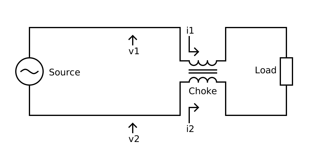
Common-mode chokes on cable exits suppress common-mode currents that would otherwise travel down cables and radiate. Source: Wikimedia Commons, CC BY-SA

Switching Power Supplies
A buck converter switching at 400 kHz does not just radiate at 400 kHz. It radiates at 400 kHz,
800 kHz, 1.2 MHz, 1.6 MHz… and harmonics keep falling above the conducted-emissions floor all the
way up through the radiated range. The 250th harmonic of a 400 kHz switcher is 100 MHz — right in
the middle of the radiated emissions band. The switching node (SW pin) is the primary radiating
structure on a typical buck converter PCB. Keep its copper area as small as possible.
Crystal Oscillators and Clock Lines
A 48 MHz USB clock radiates at 48, 96, 144, 192, 240 MHz… At some harmonic, you will hit a
frequency where the PCB trace acts as an efficient antenna. The 6th harmonic of 48 MHz is 288 MHz,
and a 26 cm trace is λ/4 at 288 MHz. If your clock line is 26 cm long, it is now a tuned antenna.
High-Speed Differential Pairs
USB 2.0, HDMI, Ethernet, PCIe — these are differential but common-mode noise (from impedance
mismatches, via stubs, return path discontinuities) still radiates. The most common real-world
failure mode: an HDMI cable of 1.5 m picks up common-mode noise at 300–500 MHz from the display
controller and re-radiates it. The product passes with a 0.5 m cable on the bench. It fails at the
test lab with a 1.5 m cable.
The Antenna Effect of Cables
A cable becomes an efficient antenna when its length approaches λ/4 at a noise frequency.
λ/4 at 100 MHz = 300 MHz·m ÷ (4 × 100 MHz) = 0.75 m
λ/4 at  50 MHz = 1.5 m
λ/4 at  30 MHz = 2.5 m
A 1-metre USB cable is λ/4 at 75 MHz. A 2-metre power cord is λ/4 at 37.5 MHz. These are
squarely in the conducted and radiated emissions measurement bands. This is why a product that looks
fine on the bench — 15 cm of cable, measured near-field with a probe — fails catastrophically at
the test lab where the required cable lengths are standardized and sometimes 1–2 m.
EMC Testing Framework
Conducted Emissions Spectrum Concept
IEC 61000-4-x Immunity Tests — Quick Reference
| Test Standard | Threat Name | Test Level (typical) | Real-World Equivalent |
|---|---|---|---|
| IEC 61000-4-2 | ESD | ±4 kV contact, ±8 kV air (Level 4) | Person touching connector after walking on carpet |
| IEC 61000-4-3 | Radiated RF immunity | 3 V/m (Level 2), 10 V/m (Level 3) | Handheld radio transmitter at 1 m |
| IEC 61000-4-4 | EFT/Burst | ±1 kV on AC port, ±0.5 kV on I/O (Level 2) | Relay or contactor switching on the same bus |
| IEC 61000-4-5 | Surge | ±1 kV line-to-line, ±2 kV line-to-earth (Level 3) | Lightning strike on outdoor cable run |
| IEC 61000-4-6 | Conducted RF immunity | 3 Vrms (Level 2), 10 Vrms (Level 3) | AM transmitter coupled onto cable |
| IEC 61000-4-8 | Power-freq magnetic | 30 A/m continuous (Level 4) | Near a large transformer or welding machine |
| IEC 61000-4-11 | Voltage dip | 0%, 40%, 70% dip for 0.5–25 cycles | Motor starting on the same mains circuit |
Pre-Compliance Habits That Save Money
- Near-field probe scan early — a $30 clamp-on current probe and a spectrum analyser (or
even an RTL-SDR) can find your worst radiating structures on the bench before you spend money at
a test lab. - Ferrite beads on cables — fit footprints for ferrite beads on every I/O line and power
input during layout. They cost ₹5 each. Removing them is free. Not having the footprint costs
you a PCB spin. - Ground pour under switching nodes — the SW node copper area on a buck converter is the
primary radiated emitter. Make it as small as it can possibly be while still handling current. - Test with full-length cables — if the product ships with a 1.5 m cable, test with a 1.5 m
cable. Not 20 cm. - Check Class B, not Class A — if there is any chance your product will be sold into
residential environments, design to Class B from day one. Retrofitting a Class A design to Class
B after certification failure is expensive.
Key Takeaway
EMC is not a stamp you apply at the end of a project — it is a series of design decisions made
during schematic capture and PCB layout. The cost of failing at a test lab is 10–100x the cost of
getting it right during design. Every switching node, every long cable, every crystal oscillator is
a potential antenna. Treat them that way from the first layout revision.